|
[ Chapter Index ] [ Next page ] CMOS LOGICA CMOS transistor (or device) has four terminals: gate , source , drain , and a fourth terminal that we shall ignore until the next section. A CMOS transistor is a switch. The switch must be conducting or on to allow current to flow between the source and drain terminals (using open and closed for switches is confusing—for the same reason we say a tap is on and not that it is closed ). The transistor source and drain terminals are equivalent as far as digital signals are concerned—we do not worry about labeling an electrical switch with two terminals.
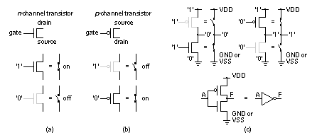
We turn a transistor on or off using the gate terminal. There are two kinds of CMOS transistors: n -channel transistors and p -channel transistors. An n -channel transistor requires a logic '1' (from now on I’ll just say a '1') on the gate to make the switch conducting (to turn the transistor on ). A p -channel transistor requires a logic '0' (again from now on, I’ll just say a '0') on the gate to make the switch nonconducting (to turn the transistor off ). The p -channel transistor symbol has a bubble on its gate to remind us that the gate has to be a '0' to turn the transistor on . All this is shown in Figure 2.1(a) and (b).
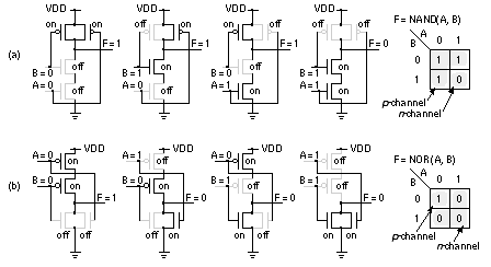
If we connect an n -channel transistor in series with a p -channel transistor, as shown in Figure 2.1(c), we form an inverter . With four transistors we can form a two-input NAND gate (Figure 2.2a). We can also make a two-input NOR gate (Figure 2.2b). Logic designers normally use the terms NAND gate and logic gate (or just gate), but I shall try to use the terms NAND cell and logic cell rather than NAND gate or logic gate in this chapter to avoid any possible confusion with the gate terminal of a transistor.
2.1 CMOS Transistors2.2 The CMOS Process2.3 CMOS Design Rules2.4 Combinational Logic Cells2.5 Sequential Logic Cells2.6 Datapath Logic Cells2.7 I/O Cells2.8 Cell Compilers2.9 Summary2.10 Problems2.11 Bibliography2.12 References |
|||||
|
|
|||||
|
|||||


