|
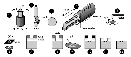
[ Chapter start ] [ Previous page ] [ Next page ] 2.2 The CMOS ProcessFigure 2.6 outlines the steps to create an integrated circuit. The starting material is silicon, Si, refined from quartzite (with less than 1 impurity in 10 10 silicon atoms). We draw a single-crystal silicon boule (or ingot) from a crucible containing a melt at approximately 1500 °C (the melting point of silicon at 1 atm. pressure is 1414 °C). This method is known as Czochralski growth. Acceptor ( p -type) or donor ( n -type) dopants may be introduced into the melt to alter the type of silicon grown. The boule is sawn to form thin circular wafers (6, 8, or 12 inches in diameter, and typically 600 m m thick), and a flat is ground (the primary flat), perpendicular to the <110> crystal axis—as a “this edge down” indication. The boule is drawn so that the wafer surface is either in the (111) or (100) crystal planes. A smaller secondary flat indicates the wafer crystalline orientation and doping type. A typical submicron CMOS processes uses p -type (100) wafers with a resistivity of approximately 10 W cm—this type of wafer has two flats, 90° apart. Wafers are made by chemical companies and sold to the IC manufacturers. A blank 8-inch wafer costs about $100. To begin IC fabrication we place a batch of wafers (a wafer lot ) on a boat and grow a layer (typically a few thousand angstroms) of silicon dioxide , SiO 2 , using a furnace. Silicon is used in the semiconductor industry not so much for the properties of silicon, but because of the physical, chemical, and electrical properties of its native oxide, SiO 2 . An IC fabrication process contains a series of masking steps (that in turn contain other steps) to create the layers that define the transistors and metal interconnect. Each masking step starts by spinning a thin layer (approximately 1 m m) of liquid photoresist ( resist ) onto each wafer. The wafers are baked at about 100 °C to remove the solvent and harden the resist before being exposed to ultraviolet (UV) light (typically less than 200 nm wavelength) through a mask . The UV light alters the structure of the resist, allowing it to be removed by developing. The exposed oxide may then be etched (removed). Dry plasma etching etches in the vertical direction much faster than it does horizontally (an anisotropic etch). Wet etch techniques are usually isotropic . The resist functions as a mask during the etch step and transfers the desired pattern to the oxide layer. Dopant ions are then introduced into the exposed silicon areas. Figure 2.6 illustrates the use of ion implantation . An ion implanter is a cross between a TV and a mass spectrometer and fires dopant ions into the silicon wafer. Ions can only penetrate materials to a depth (the range , normally a few microns) that depends on the closely controlled implant energy (measured in keV—usually between 10 and 100 keV; an electron volt, 1 eV, is 1.6 ¥ 10 –19 J). By using layers of resist, oxide, and polysilicon we can prevent dopant ions from reaching the silicon surface and thus block the silicon from receiving an implant . We control the doping level by counting the number of ions we implant (by integrating the ion-beam current). The implant dose is measured in atoms/cm 2 (typical doses are from 10 13 to 10 15 cm –2 ). As an alternative to ion implantation we may instead strip the resist and introduce dopants by diffusion from a gaseous source in a furnace. Once we have completed the transistor diffusion layers we can deposit layers of other materials. Layers of polycrystalline silicon (polysilicon or poly ), SiO 2 , and silicon nitride (Si 3 N 4 ), for example, may be deposited using chemical vapor deposition ( CVD ). Metal layers can be deposited using sputtering . All these layers are patterned using masks and similar photolithography steps to those shown in Figure 2.6.
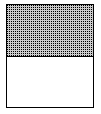
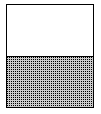
Table 2.2 shows the mask layers (and their relation to the drawn layers) for a submicron, silicon-gate, three-level metal, self-aligned, CMOS process . A process in which the effective gate length is less than 1 m m is referred to as a submicron process . Gate lengths below 0.35 m m are considered in the deep-submicron regime. Figure 2.7 shows the layers that we draw to define the masks for the logic cell of Figure 1.3. Potential confusion arises because we like to keep layout simple but maintain a “what you see is what you get” (WYSIWYG) approach. This means that the drawn layers do not correspond directly to the masks in all cases. We can construct wells in a CMOS process in several ways. In an n-well process , the substrate is p -type (the wafer itself) and we use an n -well mask to build the n -well. We do not need a p -well mask because there are no p -wells in an n -well process—the n -channel transistors all sit in the substrate (the wafer)—but we often draw the p -well layer as though it existed. In a p-well process we use a p -well mask to make the p -wells and the n -wells are the substrate. In a twin-tub (or twin-well ) process, we create individual wells for both types of transistors, and neither well is the substrate (which may be either n -type or p -type). There are even triple-well processes used to achieve even more control over the transistor performance. Whatever process that we use we must connect all the n -wells to the most positive potential on the chip, normally VDD, and all the p -wells to VSS; otherwise we may forward bias the bulk to source/drain pn -junctions. The bulk connections for CMOS transistors are not usually drawn in digital circuit schematics, but these substrate contacts ( well contacts or tub ties ) are very important. After we make the well(s), we grow a layer (approximately 1500 Å) of Si 3 N 4 over the wafer. The active mask (CAA) leaves this nitride layer only in the active areas that will later become transistors or substrate contacts. Thus the ∨ symbol represents OR (union) of the two drawn layers, ndiff and pdiff. Everything outside the active areas is known as the field region, or just field . Next we implant the substrate to prevent unwanted transistors from forming in the field region—this is the field implant or channel-stop implant . The nitride over the active areas acts as an implant mask and we may use another field-implant mask at this step also. Following this we grow a thick (approximately 5000 Å) layer of SiO 2 , the field oxide ( FOX ). The FOX will not grow over the nitride areas. When we strip the nitride we are left with FOX in the areas we do not want to dope the silicon. Following this we deposit, dope, mask, and etch the poly gate material, CPG (mask) = poly (drawn). Next we create the doped regions that form the sources, drains, and substrate contacts using ion implantation. The poly gate functions like masking tape in these steps. One implant (using phosphorous or arsenic ions) forms the n -type source/drain for the n -channel transistors and n -type substrate contacts (CSN). A second implant (using boron ions) forms the p -type source–drain for the p -channel transistors and p -type substrate contacts (CSP). These implants are masked as follows where “grow” means that we expand or bloat the drawn ndiff and drawn pdiff layers slightly (usually by a few l ). During implantation the dopant ions are blocked by the resist pattern defined by the CSN and CSP masks. The CSN mask thus prevents the n -type regions being implanted with p -type dopants (and vice versa for the CSP mask). As we shall see, the CSN and CSP masks are not intended to define the edges of the n -type and p -type regions. Instead these two masks function more like newspaper that prevents paint from spraying everywhere. The dopant ions are also blocked from reaching the silicon surface by the poly gates and this aligns the edge of the source and drain regions to the edges of the gates (we call this a self-aligned process ). In addition, the implants are blocked by the FOX and this defines the outside edges of the source, drain, and substrate contact regions. The only areas of the silicon surface that are doped n -type are
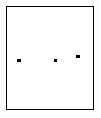
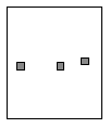
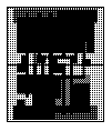
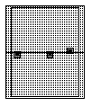
where the ∧ symbol represents AND (the intersection of two layers); and the ÿ symbol represents NOT. Similarly, the only regions that are doped p -type are
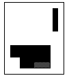
If the CSN and CSP masks do not overlap, it is possible to save a mask by using one implant mask (CSN or CSP) for the other type (CSP or CSN). We can do this by using a positive resist (the pattern of resist remaining after developing is the same as the dark areas on the mask) for one implant step and a negative resist (vice versa) for the other step. However, because of the poor resolution of negative resist and because of difficulties in generating the implant masks automatically from the drawn diffusions (especially when opposite diffusion types are drawn close to each other or touching), it is now common to draw both implant masks as well as the two diffusion layers. It is important to remember that, even though poly is above diffusion, the polysilicon is deposited first and acts like masking tape. It is rather like airbrushing a stripe—you use masking tape and spray everywhere without worrying about making straight lines. The edges of the pattern will align to the edge of the tape. Here the analogy ends because the poly is left in place. Thus,
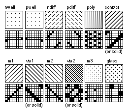
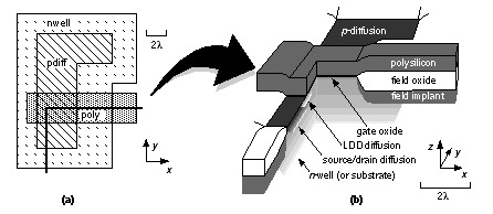
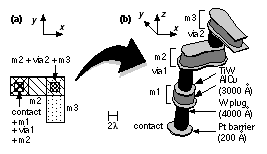
In the ASIC industry the names nplus, n +, and n -diffusion (as well as the p -type equivalents) are used in various ways. These names may refer to either the drawn diffusion layer (that we call ndiff), the mask (CSN), or the doped region on the silicon (the intersection of the active and implant mask that we call n -diffusion)—very confusing. The source and drain are often formed from two separate implants. The first is a light implant close to the edge of the gate, the second a heavier implant that forms the rest of the source or drain region. The separate diffusions reduce the electric field near the drain end of the channel. Tailoring the device characteristics in this fashion is known as drain engineering and a process including these steps is referred to as an LDD process , for lightly doped drain ; the first light implant is known as an LDD diffusion or LDD implant. Figure 2.8 shows a stipple-pattern matrix for a CMOS process. When we draw layout you can see through the layers—all the stipple patterns are OR’ed together. Figure 2.9 shows the transistor layers as they appear in layout (drawn using the patterns from Figure 2.8) and as they appear on the silicon. Figure 2.10 shows the same thing for the interconnect layers. 2.2.1 Sheet ResistanceTables 2.3 and 2.4 show the sheet resistance for each conducting layer (in decreasing order of resistance) for two different generations of CMOS process. The diffusion layers, n -diffusion and p -diffusion, both have a high resistivity—typically from 1–100 W /square. We measure resistance in W / square (ohms per square) because for a fixed thickness of material it does not matter what the size of a square is—the resistance is the same. Thus the resistance of a rectangular shape of a sheet of material may be calculated from the number of squares it contains times the sheet resistance in W / square. We can use diffusion for very short connections inside a logic cell, but not for interconnect between logic cells. Poly has the next highest resistance to diffusion. Most submicron CMOS processes use a silicide material (a metallic compound of silicon) that has much lower resistivity (at several W /square) than the poly or diffusion layers alone. Examples are tantalum silicide, TaSi; tungsten silicide, WSi; or titanium silicide, TiSi. The stoichiometry of these deposited silicides varies. For example, for tungsten silicide W:Si ª 1:2.6. There are two types of silicide process. In a silicide process only the gate is silicided. This reduces the poly sheet resistance, but not that of the source–drain. In a self-aligned silicide ( salicide ) process, both the gate and the source–drain regions are silicided. In some processes silicide can be used to connect adjacent poly and diffusion (we call this feature LI , white metal, local interconnect, metal0, or m0). LI is useful to reduce the area of ASIC RAM cells, for example. Interconnect uses metal layers with resistivities of tens of m W /square, several orders of magnitude less than the other layers. There are usually several layers of metal in a CMOS ASIC process, each separated by an insulating layer. The metal layer above the poly gate layer is the first-level metal ( m1 or metal1), the next is the second-level metal ( m2 or metal2), and so on. We can make connections from m1 to diffusion using diffusion contacts or to the poly using polysilicon contacts . After we etch the contact holes a thin barrier metal (typically platinum) is deposited over the silicon and poly. Next we form contact plugs ( via plugs for connections between metal layers) to reduce contact resistance and the likelihood of breaks in the contacts. Tungsten is commonly used for these plugs. Following this we form the metal layers as sandwiches. The middle of the sandwich is a layer (usually from 3000 Å to 10,000 Å) of aluminum and copper. The top and bottom layers are normally titanium–tungsten (TiW, pronounced “tie-tungsten”). Submicron processes use chemical–mechanical polishing ( CMP ) to smooth the wafers flat before each metal deposition step to help with step coverage. An insulating glass, often sputtered quartz (SiO 2 ), though other materials are also used, is deposited between metal layers to help create a smooth surface for the deposition of the metal. Design rules may refer to this insulator as an intermetal oxide ( IMO ) whether they are in fact oxides or not, or interlevel dielectric ( ILD ). The IMO may be a spin-on polymer; boron-doped phosphosilicate glass (BPSG); Si 3 N 4 ; or sandwiches of these materials (oxynitrides, for example). We make the connections between m1 and m2 using metal vias , cuts , or just vias . We cannot connect m2 directly to diffusion or poly; instead we must make these connections through m1 using a via. Most processes allow contacts and vias to be placed directly above each other without restriction, arrangements known as stacked vias and stacked contacts . We call a process with m1 and m2 a two-level metal ( 2LM ) technology. A 3LM process includes a third-level metal layer ( m3 or metal3), and some processes include more metal layers. In this case a connection between m1 and m2 will use an m1/m2 via, or via1 ; a connection between m2 and m3 will use an m2/m3 via, or via2 , and so on. The minimum spacing of interconnects, the metal pitch , may increase with successive metal layers. The minimum metal pitch is the minimum spacing between the centers of adjacent interconnects and is equal to the minimum metal width plus the minimum metal spacing. Aluminum interconnect tends to break when carrying a high current density. Collisions between high-energy electrons and atoms move the metal atoms over a long period of time in a process known as electromigration . Copper is added to the aluminum to help reduce the problem. The other solution is to reduce the current density by using wider than minimum-width metal lines. Tables 2.5 and 2.6 show maximum specified contact resistance and via resistance for two generations of CMOS processes. Notice that a m1 contact in either process is equal in resistance to several hundred squares of metal. [ Chapter start ] [ Previous page ] [ Next page ] | |||||||||||||||||||||||||||||||||||||||||||||||||||||||||||||||||||||||||||||||||||||||||||||||||||||||||||||||||||||||||||||||||||||||||||||||||||||||||||||||||
