2.3 CMOS Design Rules
2.3 CMOS Design Rules
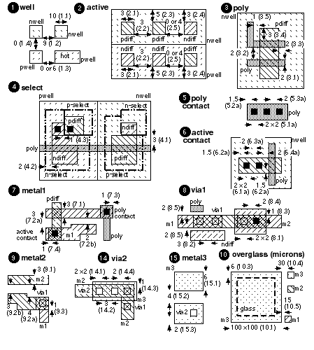
Figure 2.11 defines the
design rules
for a CMOS process using pictures. Arrows between objects denote a minimum spacing, and arrows showing the size of an object denote a minimum width. Rule 3.1, for example, is the minimum width of poly (2
l
). Each of the rule numbers may have different values for different manufacturers—there are no standards for design rules. Tables 2.7–2.9 show the MOSIS scalable CMOS rules. Table 2.7 shows the layer rules for the
process front end
, which is the front end of the line (as in production line) or
FEOL
. Table 2.8 shows the rules for the process back end (
BEOL
), the metal interconnect, and Table 2.9 shows the rules for the pad layer and glass layer.
|

|
|
FIGURE 2.11 The MOSIS scalable CMOS design rules (rev. 7). Dimensions are in
l
. Rule numbers are in parentheses (missing rule sets 11–13 are extensions to this basic process).
|
|
TABLE 2.7 MOSIS scalable CMOS rules version 7—the process front end.
|
|
Layer
|
Rule
|
Explanation
|
Value
/
l
|
|
well (CWN, CWP)
|
1.1
|
minimum width
|
10
|
|
|
1.2
|
minimum space (different potential, a hot well)
|
9
|
|
|
1.3
|
minimum space (same potential)
|
0 or 6
|
|
|
1.4
|
minimum space (different well type)
|
0
|
|
|
|
|
|
|
active (CAA)
|
2.1/2.2
|
minimum width/space
|
3
|
|
|
2.3
|
source/drain active to well edge space
|
5
|
|
|
2.4
|
substrate/well contact active to well edge space
|
3
|
|
|
2.5
|
minimum space between active (different implant type)
|
0 or 4
|
|
|
|
|
|
|
poly (CPG)
|
3.1/3.2
|
minimum width/space
|
2
|
|
|
3.3
|
minimum gate extension of active
|
2
|
|
|
3.4
|
minimum active extension of poly
|
3
|
|
|
3.5
|
minimum field poly to active space
|
1
|
|
|
|
|
|
|
select (CSN, CSP)
|
4.1
|
minimum select spacing to channel of transistor
|
3
|
|
|
4.2
|
minimum select overlap of active
|
2
|
|
|
4.3
|
minimum select overlap of contact
|
1
|
|
|
4.4
|
minimum select width and spacing
|
2
|
|
|
|
|
|
|
poly contact (CCP)
|
5.1.a
|
exact contact size
|
2
¥
2
|
|
|
5.2.a
|
minimum poly overlap
|
1.5
|
|
|
5.3.a
|
minimum contact spacing
|
2
|
|
|
|
|
|
|
active contact (CCA)
|
6.1.a
|
exact contact size
|
2
¥
2
|
|
|
6.2.a
|
minimum active overlap
|
1.5
|
|
|
6.3.a
|
minimum contact spacing
|
2
|
|
|
6.4.a
|
minimum space to gate of transistor
|
2
|
|
TABLE 2.8 MOSIS scalable CMOS rules version 7—the process back end.
|
|
Layer
|
Rule
|
Explanation
|
Value /
l
|
|
metal1 (CMF)
|
7.1
|
minimum width
|
3
|
|
|
7.2.a
|
minimum space
|
3
|
|
|
7.2.b
|
minimum space (for minimum-width wires only)
|
2
|
|
|
7.3
|
minimum overlap of poly contact
|
1
|
|
|
7.4
|
minimum overlap of active contact
|
1
|
|
via1 (CVA)
|
8.1
|
exact size
|
2
¥
2
|
|
|
8.2
|
minimum via spacing
|
3
|
|
|
8.3
|
minimum overlap by metal1
|
1
|
|
|
8.4
|
minimum spacing to contact
|
2
|
|
|
8.5
|
minimum spacing to poly or active edge
|
2
|
|
metal2 (CMS)
|
9.1
|
minimum width
|
3
|
|
|
9.2.a
|
minimum space
|
4
|
|
|
9.2.b
|
minimum space (for minimum-width wires only)
|
3
|
|
|
9.3
|
minimum overlap of via1
|
1
|
|
via2 (CVS)
|
14.1
|
exact size
|
2
¥
2
|
|
|
14.2
|
minimum space
|
3
|
|
|
14.3
|
minimum overlap by metal2
|
1
|
|
|
14.4
|
minimum spacing to via1
|
2
|
|
metal3 (CMT)
|
15.1
|
minimum width
|
6
|
|
|
15.2
|
minimum space
|
4
|
|
|
15.3
|
minimum overlap of via2
|
2
|
|
TABLE 2.9 MOSIS scalable CMOS rules version 7—the pads and overglass (passivation).
|
|
Layer
|
Rule
|
Explanation
|
Value
|
|
glass (COG)
|
10.1
|
minimum bonding-pad width
|
100
m
m
¥
100
m
m
|
|
|
10.2
|
minimum probe-pad width
|
75
m
m
¥
75
m
m
|
|
|
10.3
|
pad overlap of glass opening
|
6
m
m
|
|
|
10.4
|
minimum pad spacing to unrelated metal2 (or metal3)
|
30
m
m
|
|
|
10.5
|
minimum pad spacing to unrelated metal1, poly, or active
|
15
m
m
|
The rules in Table 2.7 and Table 2.8 are given as multiples of
l
. If we use
lambda-based rules
we can move between successive process generations just by changing the value of
l
. For example, we can scale 0.5
m
m layouts (
l
= 0.25
m
m) by a factor of 0.175 / 0.25 for a 0.35
m
m process (
l
= 0.175
m
m)—at least in theory. You may get an inkling of the practical problems from the fact that the values for pad dimensions and spacing in Table 2.9 are given in microns and not in
l
. This is because bonding to the pads is an operation that does not scale well. Often companies have two sets of design rules: one in
l
(with fractional
l
rules) and the other in microns. Ideally we would like to express all of the design rules in integer multiples of
l
. This was true for revisions 4–6, but not revision 7 of the MOSIS rules. In revision 7 rules 5.2a/6.2a are noninteger. The original Mead–Conway NMOS rules include a noninteger 1.5
l
rule for the implant layer.
[ Chapter start ] [ Previous page ] [ Next page ] | 


