|
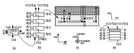
Chapter start Previous page Next page 2.6 Datapath Logic CellsSuppose we wish to build an n -bit adder (that adds two n -bit numbers) and to exploit the regularity of this function in the layout. We can do so using a datapath structure. The following two functions, SUM and COUT, implement the sum and carry out for a full adder ( FA ) with two data inputs (A, B) and a carry in, CIN: SUM = A B CIN = SUM(A, B, CIN) = PARITY(A, B, CIN),(2.38) COUT = A · B + A · CIN + B · CIN = MAJ(A, B, CIN).(2.39) The sum uses the parity function ('1' if there are an odd numbers of '1's in the inputs). The carry out, COUT, uses the 2-of-3 majority function ('1' if the majority of the inputs are '1'). We can combine these two functions in a single FA logic cell, ADD(A[ i ], B[ i ], CIN, S[ i ], COUT), shown in Figure 2.20(a), where S[ i ] = SUM(A[ i ], B[ i ], CIN),(2.40) COUT = MAJ(A[ i ], B[ i ], CIN).(2.41) Now we can build a 4-bit ripple-carry adder ( RCA ) by connecting four of these ADD cells together as shown in Figure 2.20(b). The i th ADD cell is arranged with the following: two bus inputs A[ i ], B[ i ]; one bus output S[ i ]; an input, CIN, that is the carry in from stage ( i – 1) below and is also passed up to the cell above as an output; and an output, COUT, that is the carry out to stage ( i + 1) above. In the 4-bit adder shown in Figure 2.20(b) we connect the carry input, CIN[0], to VSS and use COUT[3] and COUT[2] to indicate arithmetic overflow (in Section 2.6.1 we shall see why we may need both signals). Notice that we build the ADD cell so that COUT[2] is available at the top of the datapath when we need it. Figure 2.20(c) shows a layout of the ADD cell. The A inputs, B inputs, and S outputs all use m1 interconnect running in the horizontal directionwe call these data signals. Other signals can enter or exit from the top or bottom and run vertically across the datapath in m2we call these control signals. We can also use m1 for control and m2 for data, but we normally do not mix these approaches in the same structure. Control signals are typically clocks and other signals common to elements. For example, in Figure 2.20(c) the carry signals, CIN and COUT, run vertically in m2 between cells. To build a 4-bit adder we stack four ADD cells creating the array structure shown in Figure 2.20(d). In this case the A and B data bus inputs enter from the left and bus S, the sum, exits at the right, but we can connect A, B, and S to either side if we want. The layout of buswide logic that operates on data signals in this fashion is called a datapath . The module ADD is a datapath cell or datapath element . Just as we do for standard cells we make all the datapath cells in a library the same height so we can abut other datapath cells on either side of the adder to create a more complex datapath. When people talk about a datapath they always assume that it is oriented so that increasing the size in bits makes the datapath grow in height, upwards in the vertical direction, and adding different datapath elements to increase the function makes the datapath grow in width, in the horizontal directionbut we can rotate and position a completed datapath in any direction we want on a chip. What is the difference between using a datapath, standard cells, or gate arrays? Cells are placed together in rows on a CBIC or an MGA, but there is no generally no regularity to the arrangement of the cells within the rowswe let software arrange the cells and complete the interconnect. Datapath layout automatically takes care of most of the interconnect between the cells with the following advantages:
There are some disadvantages of using a datapath:
There are some newer standard-cell and gate-array tools that can take advantage of regularity in a design and position cells carefully. The problem is in finding the regularity if it is not specified. Using a datapath is one way to specify regularity to ASIC design tools. |
|||||
|
|
|||||
|
|||||


