|
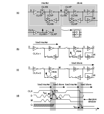
Chapter start Previous page Next page 2.5.2 Flip-FlopFigure 2.18(a) shows a flip-flop constructed from two D latches: a master latch (the first one) and a slave latch . This flip-flop contains a total of nine inverters and four TGs, or 6.5 gates. In this flip-flop design the storage node S is buffered and the clock-to-Q delay will be one inverter delay less than the clock-to-QN delay. In Figure 2.18(b) the clock input is high, the master latch is transparent, and node M (for master) will follow the D input. Meanwhile the slave latch is disconnected from the master latch and is storing whatever the previous value of Q was. As the clock goes low (the negative edge) the slave latch is enabled and will update its state (and the output Q) to the value of node M at the negative edge of the clock. The slave latch will then keep this value of M at the output Q, despite any changes at the D input while the clock is low (Figure 2.18c). When the clock goes high again, the slave latch will store the captured value of M (and we are back where we started our explanation). The combination of the master and slave latches acts to capture or sample the D input at the negative clock edge, the active clock edge . This type of flip-flop is a negative-edge–triggered flip-flop and its behavior is quite different from a latch. The behavior is shown on the IEEE symbol by using a triangular "notch" to denote an edge-sensitive input. A bubble shows the input is sensitive to the negative edge. To build a positive-edge–triggered flip-flop we invert the polarity of all the clocksas we did for a latch. The waveforms in Figure 2.18(d) show the operation of the flip-flop as we have described it, and illustrate the definition of setup time ( tSU ), hold time ( tH ), and clock-to-Q propagation delay ( tPD ). We must keep the data stable (a fixed logic '1' or '0') for a time tSU prior to the active clock edge, and stable for a time tH after the active clock edge (during the decision window shown). In Figure 2.18(d) times are measured from the points at which the waveforms cross 50 percent of V DD . We say the trip point is 50 percent or 0.5. Common choices are 0.5 or 0.65/0.35 (a signal has to reach 0.65 V DD to be a '1', and reach 0.35 V DD to be a '0'), or 0.1/0.9 (there is no standard way to write a trip point). Some vendors use different trip points for the input and output waveforms (especially in I/O cells). The flip-flop in Figure 2.18(a) is a D flip-flop and is by far the most widely used type of flip-flop in ASIC design. There are other types of flip-flopsJ-K, T (toggle), and S-R flip-flopsthat are provided in some ASIC cell libraries mainly for compatibility with TTL design. Some people use the term register to mean an array (more than one) of flip-flops or latches (on a data bus, for example), but some people use register to mean a single flip-flop or a latch. This is confusing since flip-flops and latches are quite different in their behavior. When I am talking about logic cells, I use the term register to mean more than one flip-flop. To add an asynchronous set (Q to '1') or asynchronous reset (Q to '0') to the flip-flop of Figure 2.18(a), we replace one inverter in both the master and slave latches with two-input NAND cells. Thus, for an active-low set, we replace I2 and I7 with two-input NAND cells, and, for an active-low reset, we replace I3 and I6. For both set and reset we replace all four inverters: I2, I3, I6, and I7. Some TTL flip-flops have dominant reset or dominant set , but this is difficult (and dangerous) to do in ASIC design. An input that forces Q to '1' is sometimes also called preset . The IEEE logic symbols use 'P' to denote an input with a presetting action. An input that forces Q to '0' is often also called clear . The IEEE symbols use 'R' to denote an input with a resetting action. |
|||||
|
|
|||||
|
|||||


