|
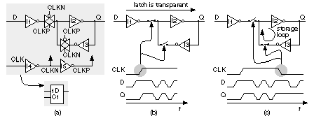
Chapter start Previous page Next page 2.5.1 LatchFigure 2.17(a) shows a sequential logic cella latch . The internal clock signals, CLKN (N for negative) and CLKP (P for positive), are generated from the system clock, CLK, by two inverters (I4 and I5) that are part of every latch cellit is usually too dangerous to have these signals supplied externally, even though it would save space. To emphasize the difference between a latch and flip-flop, sometimes people refer to the clock input of a latch as an enable . This makes sense when we look at Figure 2.17(b), which shows the operation of a latch. When the clock input is high, the latch is transparent changes at the D input appear at the output Q (quite different from a flip-flop as we shall see). When the enable (clock) goes low (Figure 2.17c), inverters I2 and I3 are connected together, forming a storage loop that holds the last value on D until the enable goes high again. The storage loop will hold its state as long as power is on; we call this a static latch. A sequential logic cell is different from a combinational cell because it has this feature of storage or memory. Notice that the output Q is unbuffered and connected directly to the output of I2 (and the input of I3), which is a storage node. In an ASIC library we are conservative and add an inverter to buffer the output, isolate the sensitive storage node, and thus invert the sense of Q. If we want both Q and QN we have to add two inverters to the circuit of Figure 2.17(a). This means that a latch requires seven inverters and two TGs (4.5 gates). The latch of Figure 2.17(a) is a positive-enable D latch, active-high D latch, or transparent-high D latch (sometimes people also call this a D-type latch). A negative-enable (active-low) D latch can be built by inverting all the clock polarities in Figure 2.17(a) (swap CLKN for CLKP and vice-versa). |
|||||
|
|
|||||
|
|||||


