


TOKYO — (BUSINESS WIRE) — January 11, 2017 — Toshiba Corporation’s (TOKYO:6502) Storage & Electronic Devices Solutions Company today announced the launch of a new line-up of low-capacitance TVS diodes [1] for use in high-speed interfaces in mobile devices, including smartphones, tablet PCs and wearable devices. The new diodes deliver the industry’s leading-class[2] protection performance. The line-up covers ten products to protect high-speed interfaces, including USB 3.0/3.1 and HDMI, from electronic discharge (ESD) and noise. Shipments start from today.
This Smart News Release features multimedia. View the full release here: http://www.businesswire.com/news/home/20170111005441/en/
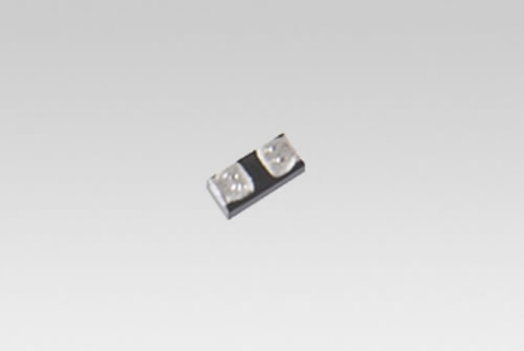
Toshiba: Low-capacitance TVS Diode for High-speed Interfaces in Mobile Devices Delivering the Industry's Leading-class Protection Performance (Photo: Business Wire)
The new series offers five products for 3.3V lines and five for 5.0V lines, allowing users to select the product that matches the required interface voltage of their system. The TVS diodes are fabricated with a newly developed EAP-IV process[3], which utilizes Toshiba’s proprietary snapback technology. It improves dynamic resistance, which absorbs ESD and noise, by approximately 50% compared to Toshiba current products[4], realizing a low clamping voltage. Furthermore, static electricity tolerance is improved by approximately 75% against Toshiba’s current products[4], which can contribute to improvements in system reliability.
Also, depending on the mounting space of sets, users have a choice of three packages. “SOD-962 (SL2)” (0.62 x 0.32mm) and “SOD-882(CST2)” (1.0 x 0.6mm) are small-size packages suited for multi-ports including the increasingly adopted USB Type-C™. The flow-through “DFN10” package (2.5 x 1.0mm) reduces the inductance that occurs from wiring.
|
Line-up and Main Specifications |
||||||||||||||||
|
(@Ta=25 ℃) |
||||||||||||||||
| Part Number | Configuration |
Absolute
|
VRWM
|
RDYN typ.
|
VC typ. (V) |
Ct typ.
|
Package | |||||||||
|
VESD
(kV) |
@16 A | @30 A | ||||||||||||||
| DF2B5M4SL | Bi-directional | ±20 | 3.6 | 0.5 | 17 | 24 | 0.2 | SOD-962 | ||||||||
| DF2B5M4CT | SOD-882 | |||||||||||||||
| DF2S5M4SL | Uni-directional | 0.3 | 14 | 18.5 | 0.35 | SOD-962 | ||||||||||
| DF2S5M4CT | SOD-882 | |||||||||||||||
| DF10G5M4N | Bi-directional | 0.5 | 17 | 24 | 0.2 | DFN10 | ||||||||||
| DF2B6M4SL | 5.5 | 0.5 | 18 | 25 | 0.2 | SOD-962 | ||||||||||
| DF2B6M4CT | SOD-882 | |||||||||||||||
| DF2S6M4SL | Uni-directional | 0.3 | 14 | 18 | 0.35 | SOD-962 | ||||||||||
| DF2S6M4CT | SOD-882 | |||||||||||||||
| DF10G6M4N | Bi-directional | 0.5 | 18 | 25 | 0.2 | DFN10 | ||||||||||


 Animation, 3D Art and 3D Models")