Delivering 5x more I/O bandwidth, up to 20x lower latency and 5x more power efficiency than current generation offerings1, and enabling new disaggregated system and memory architectures for HPC and AI
SANTA CLARA, Calif. — (BUSINESS WIRE) — November 8, 2023 — Ayar Labs, a leader in silicon photonics for chip-to-chip connectivity, will showcase its in-package optical I/O solution integrated with Intel’s industry-leading Agilex® Field-Programmable Gate Array (FPGA) technology. In demonstrating 5x current industry bandwidth at 5x lower power and 20x lower latency, the optical FPGA – packaged in a common PCIe card form factor – has the potential to transform the high performance computing (HPC) landscape for data-intensive workloads such as generative artificial intelligence (AI), machine learning, and support novel new disaggregated compute and memory architectures and more.
This press release features multimedia. View the full release here: https://www.businesswire.com/news/home/20231108423376/en/

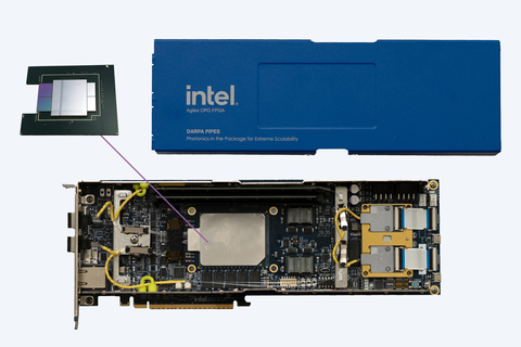
Integration of Ayar Labs TeraPHY™ optical I/O chiplets and SuperNova™ light sources into the same package with an Intel FPGA, delivered in a standard PCIe card form factor (Photo: Business Wire)
“We’re on the cusp of a new era in high performance computing as optical I/O becomes a ‘must have’ building block for meeting the exponentially growing, data-intensive demands of emerging technologies like generative AI,” said Charles Wuischpard, CEO of Ayar Labs. “Showcasing the integration of Ayar Labs’ silicon photonics and Intel’s cutting-edge FPGA technology at Supercomputing is a concrete demonstration that optical I/O has the maturity and manufacturability needed to meet these critical demands.”
At the upcoming Supercomputing 2023 conference on Nov. 12-17 in Denver, Ayar Labs will showcase an optical FPGA consisting of two TeraPHY™ optical I/O chiplets that are each capable of 4 Tbps bi-directional bandwidth. These chiplets are connected to a 10 nm FPGA fabric die, the core fabric used in Intel’s Agilex FPGAs. The optical communication is powered by two SuperNova™ light sources, supporting 64 optical channels of high-speed, error-free communication across eight fibers on each chiplet. This configuration is capable of delivering 5x the bandwidth at a fraction of the power (<5pJ/b) and latency (5ns per chiplet + TOF) required by current industry solutions, all critical factors for the future of high performance compute fabrics and next generation disaggregated architectures.
“At Intel, we pursue relentless innovation with our FPGA portfolio. With Ayar Labs’ in-package optics coupled with our FPGA fabric die, we created I/O bandwidth over 4 Tbps — far greater than what is currently possible with electrical connections,” said Venkat Yadavalli, Intel Corporation’s VP and GM, Product Excellence Group. “We’re looking well beyond 400G Ethernet with this capability. Optical interfaces like these have the potential to unlock huge advancements in high performance computing, AI, data centers, sensing, communications, edge, and more. Imagine what you could do with an optical interface FPGA communicating at over 4 Terabits per second.”
This is a great example of the benefits of the emerging chiplet ecosystem, combining Ayar Labs’ optical I/O chiplets developed on GlobalFoundries’ Fotonix™ monolithic silicon photonics platform with Intel’s FPGA and leading packaging process into a single package. This co-packaged integration has delivered a step function in performance without changing the underlying compute silicon.
The innovative optical FPGA is the latest milestone in Ayar Labs’ long-term roadmap of breakthrough performance, industry standard UCIe and CXL connections, strategic partnerships, assembly and test options for manufacturing, and many other technical and ecosystem advances.
Optical Interconnect to Address the Future of HPC and AI Application Performance
Optical I/O advances the performance and power trajectories of system designs by enabling compute, memory and networking ASICs to communicate with dramatically increased bandwidth, at a lower latency, and at a fraction of the power of existing electrical interfaces and optical interconnects. The technology is also foundational to enabling emerging disaggregated, pooled designs, heterogeneous compute systems, and unified memory architectures that are critical to accelerating future innovation.
A recent study by Hyperion Research found that users and vendors agree optical I/O is expected to be the highest impact technology to address HPC system architecture challenges over both the immediate (next two years) and near (four to six-year) term. The study also found that 79% of HPC system and semiconductor vendors surveyed believe that disaggregation and composability of system resources will be a requirement of future systems, pointing to the need for optical I/O connectivity to support these new architectures.
Ayar Labs at Supercomputing 2023:
- Experience the 4 Tbps optical FPGA with Ayar Labs’ in-package optical I/O solution in booth #228
- Panel: “Chiplet Ecosystem in High Performance Computing, AI/ML, and Data Acceleration,” including LK Bhupathi, VP of Product, Strategy, and Ecosystem, Ayar Labs, from 3:30 – 5 p.m. on Wednesday, Nov. 15
- Panel: “Scalable and Adaptable Architectures for AI/HPC Advancement,” including Vladimir Stojanovic, Co-founder and Chief Architect, Ayar Labs, from 1:30 – 3 p.m. on Thursday, Nov. 16
- A full list of Ayar Labs’ activities at SC23 is available on the Ayar Labs website
About Ayar Labs
Ayar Labs is using light to disrupt traditional compute power and performance curves, enabling the next design breakthroughs for the growth of generative AI, disaggregated data centers, 6G, phased array sensory systems and more. Ayar Labs’ patented approach uses silicon photonics techniques to replace traditional electrical-based I/O with high-speed, highly efficient, low-latency optical interconnect chiplets and multi-wavelength light sources. The company was founded in 2015 and is funded by a number of domestic and international venture capital firms, as well as strategic investors such as GlobalFoundries, Hewlett Packard Pathfinder, Intel Capital, Lockheed Martin Ventures and NVIDIA. For more information, visit www.ayarlabs.com.
1 Compared with 400G pluggable optical transceivers
View source version on businesswire.com: https://www.businesswire.com/news/home/20231108423376/en/
Contact:
Kristine Raabe, press@ayarlabs.com


