Highlights:
- Cerebrus uses unique ML technology to drive the Cadence RTL-to-signoff implementation flow, delivering up to 10X productivity and 20% PPA improvements for implementation
- Built with a re-usable and transportable reinforced learning model that increases effectiveness with each use
- Provides more efficient on-site and cloud compute resource management capabilities than traditional human-driven design exploration
- Improves PPA and productivity across many nodes and multiple end-applications including consumer, hyperscale computing, 5G communications, automotive and mobile design
SAN JOSE, Calif. — (BUSINESS WIRE) — July 22, 2021 — Cadence Design Systems, Inc. (Nasdaq: CDNS) today announced the delivery of the Cadence® Cerebrus™ Intelligent Chip Explorer, a new machine learning (ML)-based tool that automates and scales digital chip design, enabling customers to efficiently achieve demanding chip design goals. The combination of Cerebrus and the Cadence RTL-to-signoff flow offers advanced chip designers, CAD teams and IP developers the ability to improve engineering productivity by up to 10X versus a manual approach while also realizing up to a 20% better power, performance and area (PPA).
This press release features multimedia. View the full release here: https://www.businesswire.com/news/home/20210722005331/en/

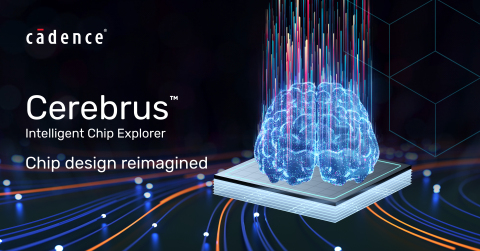
The Cadence® Cerebrus™ Intelligent Chip Explorer is a new machine learning (ML)-based tool that automates and scales digital chip design, enabling customers to efficiently achieve demanding chip design goals. (Graphic: Business Wire)
With the addition of Cerebrus to the broader digital product portfolio, Cadence offers the industry’s most advanced ML-enabled digital full flow, from synthesis through implementation and signoff. The new tool is cloud enabled and utilizes highly scalable compute resources from leading cloud providers to rapidly meet design requirements across a wide range of markets including consumer, hyperscale computing, 5G communications, automotive and mobile. For more information on Cerebrus, please visit www.cadence.com/go/cerebruspr.
Cerebrus provides customers with the following benefits:
- Reinforcement ML: Quickly finds flow solutions human engineers might not naturally try or explore, improving PPA and productivity.
- ML model reuse: Allows design learnings to be automatically applied to future designs, reducing the time to better results.
- Improved productivity: Lets a single engineer optimize the complete RTL-to-GDS flow automatically for many blocks concurrently, allowing full design teams to be more productive.
- Massively distributed computing: Provides scalable on-premises or cloud-based design exploration for faster flow optimization.
- Easy-to-use interface: Powerful user cockpit allows interactive results analytics and run management to gain valuable insights into design metrics.
“Previously, design teams didn’t have an automated way to reuse historical design knowledge, leading to excess time spent on manual re-learning with each new project and lost margins,” said Dr. Chin-Chi Teng, senior vice president and general manager in the Digital & Signoff Group at Cadence. “The delivery of Cerebrus marks an EDA industry revolution with ML-driven digital chip design where engineering teams have a greater opportunity to provide higher impact in their organizations because they can offload manual processes. As the industry continues to move to advanced nodes and design size and complexity increase, Cerebrus lets designers achieve PPA goals much more efficiently.”
Cerebrus is part of the broader Cadence digital full flow, working seamlessly with the Genus™ Synthesis Solution, Innovus™ Implementation System, Tempus™ Timing Signoff Solution, Joules™ RTL Power Solution, Voltus™ IC Power Integrity Solution and Pegasus™ Verification System to provide customers with a fast path to design closure and better predictability. The new tool and the broader flow support the company’s Intelligent System Design™ strategy, which enables pervasive intelligence for design excellence.
Customer Endorsements
“To efficiently maximize the performance of new products that use emerging process nodes, digital implementation flows used by our engineering team need to be continuously updated. Automated design flow optimization is critical for realizing product development at a much higher throughput. Cerebrus, with its innovative ML capabilities, and the Cadence RTL-to-signoff tools have provided automated flow optimization and floorplan exploration, improving design performance by more than 10%. Following this success, the new approach will be adopted in the development of our latest design projects.”
- Satoshi Shibatani, director, Digital Design Technology Department, Shared R&D EDA Division, Renesas
“As Samsung Foundry continues to deploy up-to-date process nodes, the efficiency of our Design Technology Co-Optimization (DTCO) program is very important, and we are always looking for innovative ways to exceed PPA in chip implementation. As part of our long-term partnership with Cadence, Samsung Foundry has used Cerebrus and the Cadence digital implementation flow on multiple applications. We’ve observed more than an 8% power reduction on some of our most critical blocks in just a few days versus many months of manual effort. In addition, we are using Cerebrus for automated floorplan power distribution network sizing, which has resulted in more than 50% better final design timing. Due to Cerebrus and the digital implementation flow delivering better PPA and significant productivity improvements, the solution has become a valuable addition to our DTCO program.”
- Sangyun Kim, vice president, Design Technology, Samsung Foundry
About Cadence
Cadence is a pivotal leader in electronic design, building upon more than 30 years of computational software expertise. The company applies its underlying Intelligent System Design strategy to deliver software, hardware and IP that turn design concepts into reality. Cadence customers are the world’s most innovative companies, delivering extraordinary electronic products from chips to boards to systems for the most dynamic market applications, including consumer, hyperscale computing, 5G communications, automotive, mobile, aerospace, industrial and healthcare. For seven years in a row, Fortune magazine has named Cadence one of the 100 Best Companies to Work For. Learn more at
cadence.com.
© 2021 Cadence Design Systems, Inc. All rights reserved worldwide. Cadence, the Cadence logo and the other Cadence marks found at www.cadence.com/go/trademarks are trademarks or registered trademarks of Cadence Design Systems, Inc. All other trademarks are the property of their respective owners.
View source version on businesswire.com: https://www.businesswire.com/news/home/20210722005331/en/
Contact:
For more information, please contact:
Cadence Newsroom
408-944-7039
newsroom@cadence.com


