


Samsung starts shipping industry's first third-gen 10nm-class (1z) EUV-based 16Gb LPDDR5 DRAM
Following DRAM, new Pyeongtaek Line 2 to produce next-gen V-NAND and foundry solutions
SEOUL, South Korea — (BUSINESS WIRE) — August 31, 2020 — Samsung Electronics Co., Ltd., the world leader in advanced memory technology, today announced that its second production line in Pyeongtaek, Korea, has commenced mass production of the industry's first 16-gigabit (Gb) LPDDR5 mobile DRAM, using extreme ultraviolet (EUV) technology. Built on Samsung's third-generation 10nm-class (1z) process, the new 16Gb LPDDR5 boasts the highest mobile memory performance and largest capacity to enable more consumers to enjoy the full benefits of 5G and AI features in next-generation smartphones.
This press release features multimedia. View the full release here: https://www.businesswire.com/news/home/20200831005214/en/
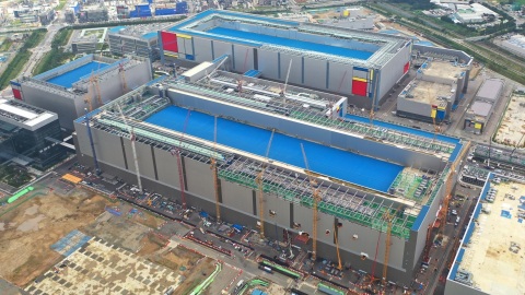
Samsung Pyeongtaek line 2, the largest-scale semiconductor production line (Photo: Business Wire)
"The 1z-based 16Gb LPDDR5 elevates the industry to a new threshold, overcoming a major developmental hurdle in DRAM scaling at advanced nodes," said Jung-bae Lee, executive vice president of DRAM Product & Technology at Samsung Electronics. "We will continue to expand our premium DRAM lineup and exceed customer demands, as we lead in growing the overall memory market."
Expanding Manufacturing Capacity in Pyeongtaek Complex
Spanning more than 128,900 square meters (over 1.3 million square feet) – equivalent to about 16 soccer fields – Samsung's Pyeongtaek Line 2 is the largest-scale semiconductor production line to date.
The new Pyeongtaek line will serve as the key manufacturing hub for the industry’s most advanced semiconductor technologies, delivering cutting-edge DRAM followed by next-generation V-NAND and foundry solutions, while reinforcing the company's leadership in the Industry 4.0 era.
Fastest, Largest-capacity Mobile Memory
Based on today's most advanced (1z) process node, Samsung’s new 16Gb LPDDR5 is the first memory to be mass produced using EUV technology, providing the highest speed and largest capacity available in mobile DRAM.
At 6,400 megabits per second (Mb/s), the new LPDDR5 is about 16 percent faster than the 12Gb LPDDR5 (5,500Mb/s) found in most of today's flagship mobile devices. When made into a 16GB package, the LPDDR5 can transfer about 10 5GB-sized full-HD movies, or 51.2GB of data, in one second.
Thanks to its use of the first commercial 1z process, the LPDDR5 package is 30 percent thinner than its predecessor, enabling 5G and multi-camera smartphones as well as foldable devices to pack more functionality into a slim design. The 16Gb LPDDR5 can build a 16GB package with only eight chips, whereas its 1y-based predecessor requires 12 chips (eight 12Gb chips and four 8Gb chips) to provide the same capacity.
By delivering the first 1z-based 16GB LPDDR5 to global smartphone makers, Samsung plans to further strengthen its presence in the flagship mobile device market throughout 2021. Samsung will also expand the use of its LPDDR5 offerings into automotive applications, offering an extended temperature range to meet strict safety and reliability standards in extreme environments.
About Samsung Electronics Co., Ltd.
Samsung inspires the world and shapes the future with transformative ideas and technologies. The company is redefining the worlds of TVs, smartphones, wearable devices, tablets, digital appliances, network systems, and memory, system LSI, foundry and LED solutions. For the latest news, please visit the Samsung Newsroom at http://news.samsung.com.
View source version on businesswire.com: https://www.businesswire.com/news/home/20200831005214/en/
Contact:
Ujeong Jahnke
Samsung Semiconductor Europe GmbH
Tel. +49(0)6196-66-3300
Email:
ujeong.j@samsung.com


 Animation, 3D Art and 3D Models")