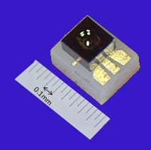
KP-H KPDEH12L-CC1C with 400Gbps transmission speed will begin mass production in November, 2020
TOKYO — (BUSINESS WIRE) — June 28, 2020 — Kyoto Semiconductor Co., Ltd. (headquartered in Kyoto, Japan) has developed a high-speed photodiode KP-H KPDEH12L-CC1C to support 400Gbps transmission systems that use PAM4 (Pulse Amplitude Modulation 4) inside and between data centers. With the introduction of this InGaAs photodiode, the company is continually supporting the increasing speeds and capacity requirements for transmission systems in 5G networks and beyond. Mass production will start in November, 2020.
This press release features multimedia. View the full release here: https://www.businesswire.com/news/home/20200628005047/en/

KP-H High-speed Photodiode KPDEH12L-CC1C (Graphic: Business Wire)
KP-H KPDEH12L-CC1C main features
(1) High-speed
The size of the carrier on which the PD is mounted, and the width and length of the high frequency electrode pattern placed on the carrier are optimized using an electromagnetic simulation (Note 2). As a result, we have achieved the world’s top class 400Gbps and 40GHz as a frequency band with an integrated transimpedance amplifier. The KP-H photodiode has passed Telcordia GR-468-Core, which is the standard reliability test for communication equipment.
(2) Easy implementation
KPDEH12L-CC1C is mounted on a carrier that is optimally designed to achieve high frequency. A condenser lens is integrated on the backside of the photodiode (Note 3), allowing the incoming light to collect in the light absorption area, and makes it easy to align the optical fiber with PD. The PD chip is mounted on a carrier twice as big as the chip itself.
Background of development
Currently, we have achieved transmission speeds of mainly 100Gbps by bundling 4 lanes of 25Gbps. However, there are growing demands in the market for 400Gps to 800Gbps transmission speeds. The Institute of Electrical and Electronics Engineers (IEEE) set the standard of PAM4 that corresponds with 4-bit signal to one modulation. The transmission speed per PD reaches 50Gps (= 400Gps/4 lanes/2 (PAM4)). The transmission bandwidth required for the PD to achieve this speed will be 35~40GHz.
See the following for more information. https://www.kyosemi.co.jp/en/lp/kpdeh12l-cc1c
About Kyoto Semiconductor
Kyoto Semiconductor was established in 1980 in Kyoto as a dedicated manufacturer of semiconductors. The semiconductors manufactured offer superlative performance and precision, suited for use in optical transmission. They are manufactured end-to-end, including pre- and post-processing, and together with Kyoto Semiconductor’s unique packaging technology, at our location in Japan and made available to customers around the world. Kyoto Semiconductor leads the industry with world-standard technologies for optical device solutions based on Japanese quality and attention to production detail.
Notes
1) 4- level modulation method 8PAM 4 (Pulse Amplitude Modulation 4)
Instead of mounting 2-bit information {0, 1} for one modulation, the method mounts 4-bit information {0, 1, 2, 3}. This method allows transmission of twice as much information as conventional method.
2) Carrier
The patterns with little attenuation in the high-frequency are formulated on the surface of the board on which the PD is mounted. The dimension of the carrier is 0.6 x 0.48 x 0.25 t mm.
3) Condenser lens
The figure shows a schematic view of the PD chip. A condenser lens is built into the surface where the light enters, and is focused and collected on a small light absorption layer.
© 2020 Kyoto Semiconductor, Co Ltd. All rights reserved. Information in this press release, including product pricing and specifications, content of services, and contact information is current and believed to be accurate on the date of the announcement, but is subject to change without prior notice. Technical and application information contained here is subject to the most recent applicable Kyoto Semiconductor product specifications.
View source version on businesswire.com: https://www.businesswire.com/news/home/20200628005047/en/
Contact:
Kyoto Semiconductor Co., Ltd.
Naoko Kodama, Media Relations
Tel: +81-3-5312-5361
Email:
media_relation@kyosemi.co.jp


