Highlights:
- The CloudBurst platform, the latest addition to the Cadence Cloud portfolio, provides customers with fast and easy access to pre-installed Cadence design tools in a ready-to-use cloud environment built on either Amazon Web Services or Microsoft Azure
- Customers can now strategically complement their on-premises infrastructure with the massive scalability of the cloud to address the peak requirements of critical design projects
- The CloudBurst platform provides customers with secure, web-based access to a cloud environment tailored to address challenges associated with compute-intensive workloads and massive file sizes of today’s ICs and electronic systems
SAN JOSE, Calif. — (BUSINESS WIRE) — April 1, 2019 — Cadence Design Systems, Inc. (NASDAQ: CDNS) today announced the availability of the new Cadence® CloudBurst™ Platform for hybrid cloud environments, providing customers with fast and easy access to pre-installed Cadence design tools in a ready-to-use cloud environment built on either Amazon Web Services (AWS) or Microsoft Azure. The new platform is the latest addition to the Cadence Cloud portfolio, and this continued innovation further advances Cadence’s leadership position in cloud-based offerings for semiconductor and electronic system design. For more information on the new Cadence CloudBurst platform, please visit www.cadence.com/go/cloudburst.
This press release features multimedia. View the full release here: https://www.businesswire.com/news/home/20190401005241/en/

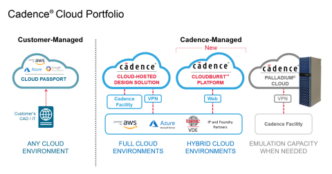
Part of the broader Cadence Cloud portfolio, the new Cadence CloudBurst Platform for hybrid cloud environments provides customers with fast and easy access to pre-installed Cadence design tools in a ready-to-use cloud environment built on either Amazon Web Services (AWS) or Microsoft Azure. (Graphic: Business Wire)
The Cadence CloudBurst platform enables companies of all sizes to build upon the standard benefits of the broader Cadence Cloud portfolio—improved productivity, scalability, security and flexibility—with a deployment option that delivers a hybrid cloud environment in just a day or two after initial purchase versus the typical timeframes for internally provided cloud solutions that can take weeks to deploy. It offers customers a production-proven, Cadence-managed environment for compute-intensive EDA workloads with no tool installation or cloud set-up required so that engineers can stay focused on completing critical, revenue-generating design projects.
Additional benefits systems and semiconductor companies can achieve with the Cadence CloudBurst platform include:
- Ability to address today’s design challenges: The platform provides convenient and secure browser-based access to the scale of cloud computing options and includes unique file-transfer technology that significantly accelerates the transfer speed of the massive files created by today’s complex system-on-chip (SoC) designs
- Ease of deployment: The platform complements existing on-premises datacenter investments and enables CAD and IT teams to easily address peak needs by providing a hybrid environment without requiring prior cloud expertise
- Access to a broad set of Cadence tools: The platform supports a range of cloud-ready tools including functional verification, circuit simulation, library characterization and signoff tools, which benefit from cloud-scale compute resources
- Streamlined ordering process: Customers can utilize existing ordering and licensing systems, eliminating sometimes lengthy legal and administrative hassles so customers can begin using the cloud for design projects quickly
“Our vision is to continuously evolve our cloud offerings to remove barriers to adoption and make customers successful in their shift to the cloud regardless of legacy investments or level of cloud experience,” said Dr. Anirudh Devgan, president of Cadence. “By adding the CloudBurst platform to our Cadence Cloud portfolio, we’re providing customers with an unparalleled offering for hybrid cloud environments, which lets customers harness the full power of the cloud for SoC development.”
The broader Cadence Cloud portfolio consists of the new CloudBurst platform as well as the customer-managed Cloud Passport model and the Cadence-managed Cloud-Hosted Design Solution and Palladium® Cloud solutions. The Cadence-managed offerings provide customers with solutions that fully support TSMC’s Open Innovation Platform Virtual Design Environment (OIP VDE). The portfolio offerings support the broader Cadence System Design Enablement strategy, which enables systems and semiconductor companies to create complete, differentiated end products more efficiently.
Endorsements
“We successfully ran more than 500 million instances flat using the
fully distributed Cadence Tempus Timing Signoff Solution on the
CloudBurst platform via AWS to complete the tapeout of our latest TSMC
7nm networking chip. This would have been impossible to achieve in the
required timeframe if we hadn’t deployed the Cadence hybrid cloud
solution, which offered quick and easy access to the massive compute
power we needed and a 10X productivity improvement over an on-premises
static timing analysis approach for final signoff.”


