Leading-Edge Process Technology Supports Data Storage, Computational Demands of Increasingly Complex Automotive Infotainment Applications
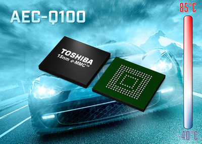
LAS VEGAS, Jan. 5, 2016 — (PRNewswire) — This week at the 2016 International CES, Toshiba America Electronic Components, Inc. (TAEC)*, a committed leader that collaborates with technology companies to create breakthrough designs, has introduced its 15nm e-MMCTM [1] NAND Flash memory for automotive applications. Toshiba's Automotive e-MMC features a wide operating temperature range of -40 to 85oC, the smallest class chip size available for Automotive [2], an 11.5x13mm JEDEC standard package, and high reliability.
Toshiba's new line-up of single-package embedded NAND flash memories is extremely well-suited to the demanding requirements of the automotive infotainment market, and includes densities from 8 gigabyte[3] (GB) to 64GB. Each device integrates a controller to manage basic control functions for NAND applications.
According to industry analyst firm Gartner, the majority of vehicles will be connected to the Internet in just five years, with 60 to 75 percent of them being capable of consuming, creating and sharing Web-based data[4]. From maps and weather conditions to voice recognition, entertainment, driver assist features and more - cars are quickly becoming much more than just modes of transportation. Accelerated processing power and increased data storage capacity are crucial to enabling all of this connectivity, and Toshiba's e-MMC NAND Flash memory has emerged as the data storage technology of choice for automotive applications.
Toshiba's 15nm chips used for e-MMC are among the world's smallest. Fully compliant with the latest JEDEC e-MMC standard, the chips are designed for application in a wide range of digital products, including automotive infotainment and industrial applications. Toshiba's 15nm e-MMC offers fast read/write performance due to improvements in basic chip performance and controller optimization.
"As the inventors of NAND Flash and a leader in NAND Flash process migrations, Toshiba continues to harness this expertise for the automotive sector with the introduction of our 15nm e-MMC for this application," noted Scott Beekman, director of managed NAND memory products for TAEC. "Our expertise in developing the industry's most innovative NAND memory products positions us perfectly to produce the high quality, high performance memory necessary for in-vehicle infotainment systems."
Key features include:
- Extended temperature range: -40 to 85oC
- Low failure rate to support higher quality demands for automotive applications
- Meets AEC-Q100 specifications
- Adheres to PPAP requirements
- Extended support
Outline of the New Products
|
Part Number |
Density |
Operating Temperature Range |
Package Size |
Mass Production |
|
THGBMHG6C1LBAAL |
8GB |
-40oC to 85oC |
11.5x13x0.8mm |
2Q(Apr.-Jun.) 2016 |
|
THGBMHG7C2LBAAR |
16GB |
-40oC to 85oC |
11.5x13x1.0mm |
2Q(Apr.-Jun.) 2016 |
|
THGBMHG8C4LBAAR |
32GB |
-40oC to 85oC |
11.5x13x1.0mm |
2Q(Apr.-Jun.) 2016 |
|
THGBMHG9C8LBAAG |
64GB |
-40oC to 85oC |
11.5x13x1.2mm |
2Q(Apr.-Jun.) 2016 |
Sample shipments are available with additional densities to follow. For more information, please visit toshiba.com/taec/adinfo/technologymoves/ and follow the company on Facebook.
|
Notes
|
|
|
Maximum read and write speed may vary depending on the host device, read and write conditions, and file size. For purposes of measuring read and write speed in this context, 1 megabyte or MB = 1,000,000 bytes. |
|
*About Toshiba Corp. and TAEC
About TAEC
Through proven commitment, lasting relationships and advanced, reliable electronic components, Toshiba enables its customers to create market-leading designs. Toshiba is the heartbeat within product breakthroughs from OEMs, ODMs, CMs, VARs, distributors and fabless chip companies worldwide. A committed electronic components leader, Toshiba designs and manufactures high-quality flash memory-based storage solutions, solid state drives (SSDs), hard disk drives (HDDs), solid state hybrid drives (SSHDs), discrete devices, custom SoCs/ASICs, imaging products, microcontrollers, wireless components, mobile peripheral devices, advanced materials and medical tubes that make possible today's leading smartphones, tablets, cameras, medical devices, automotive electronics, industrial applications, enterprise solutions and more.
Toshiba America Electronic Components, Inc. is an independent operating company owned by Toshiba America, Inc., a subsidiary of Toshiba Corporation, Japan's largest semiconductor manufacturer and the world's sixth largest semiconductor manufacturer (Gartner, 2014 Worldwide Semiconductor Revenue Estimates, December 2014 ). Founded in Tokyo in 1875, Toshiba is at the heart of a global network of over 590 consolidated companies employing over 200,000 people worldwide. Visit Toshiba's web site at
www.toshiba.co.jp/index.htm .


