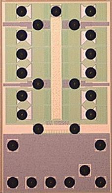
Samples fabricated with the next generation TaRF8 process to be available in January
TOKYO — (BUSINESS WIRE) — November 19, 2015 — Toshiba Corporation’s (TOKYO:6502) Semiconductor & Storage Products Company today announced the development of “TaRF8”, a next generation TarfSOI™ (Toshiba advanced RF SOI) process optimized for radio-frequency (RF) switch applications that achieves the lowest-class[1] of insertion loss[2] in the industry. Sample shipments of SP12T[3] RF switch ICs for smartphones fabricated with the new process will start in January 2016.
This Smart News Release features multimedia. View the full release here: http://www.businesswire.com/news/home/20151119006843/en/

Toshiba: RF Switch IC Fabricated with the Next Generation SOI Process Achieving the Lowest-class Insertion Loss in the Industry (Photo: Business Wire)
SP12T, a transmit RF switch IC with an integrated MIPI-RFFE[4] controller for mobile applications, is suited to the 3GPP GSM, UMTS, W-CDMA, LTE and LTE-Advanced[5] standards. Products utilizing TaRF8, the next generation process of Toshiba’s proprietary SOI-CMOS[6] TarfSOI front-end process optimized for RF switches, achieves the lowest-class insertion loss in the industry, 0.32dB at 2.7GHz. Compared with products using Toshiba’s current TaRF6 process, insertion loss is improved by 0.1dB while maintaining the same level of distortion characteristics.
With the trend in mobile communications towards high-data-rate, high-capacity data transfers, RF switch ICs used in mobile devices, including smartphones, require multi-port support and improved RF performance. Lowering insertion loss is recognized as a particularly important factor in this, as it decreases RF transmission power loss, which can support a longer battery life for mobile devices.
Toshiba is developing high-performance RF switch ICs utilizing its in-house fab to apply SOI-CMOS technology, which is suitable for integrating analog and digital circuits. By handling all aspects of the production flow, from RF process technology development to the design and manufacturing of RF switch chips, Toshiba can swiftly improve SOI-CMOS process technology in response to feedback from the development results of its own RF switch IC products. This Integrated-Device-Manufacturer (IDM) approach allows Toshiba to quickly establish new process technologies suited to actual products and to enter the market with products fabricated with the latest process technology.
Toshiba will continue improving the performance of its TarfSOI process technology and work towards meeting customer and market requirements for RF switch ICs by introducing cutting-edge technology products ahead of other manufacturers.
Notes
[1] In the RF switch IC market as of November 20, 2015.
Toshiba survey.
[2] Power loss that occurs when an RF signal is
transmitted through the switch, expressed in decibels (dB).
[3]
Single Pole Twelve Throw Switch
[4] A serial bus interface
specification for the control of RF components for mobile devices,
standardized by the RF Frontend (RFFE) Working Group of the MIPI (Mobile
Industry Processor Interface) Alliance.
[5] Mobile communication
standards specified by the 3GPP (3rd Generation Partnership Project).
[6]
Technology to reduce parasitic capacitance by using an insulation layer
under the channel of the MOSFET. SOI: Silicon-On-Insulator
* TarfSOI is a trademark of Toshiba Corporation.
Customer Inquiries:
Small Signal Device Sales & Marketing Department
Tel:
+81-3-3457-3946
Information in this document, including product prices and specifications, content of services and contact information, is current on the date of the announcement but is subject to change without prior notice.
About Toshiba
Toshiba Corporation, a Fortune Global 500 company, channels world-class capabilities in advanced electronic and electrical product and systems into five strategic business domains: Energy & Infrastructure, Community Solutions, Healthcare Systems & Services, Electronic Devices & Components, and Lifestyles Products & Services. Guided by the principles of The Basic Commitment of the Toshiba Group, “Committed to People, Committed to the Future”, Toshiba promotes global operations and is contributing to the realization of a world where generations to come can live better lives.
Founded in Tokyo in 1875, today’s Toshiba is at the heart of a global
network of over 580 consolidated companies employing 199,000 people
worldwide, with annual sales surpassing 6.6 trillion yen (US$55 billion).
To
find out more about Toshiba, visit
www.toshiba.co.jp/index.htm
View source version on businesswire.com: http://www.businesswire.com/news/home/20151119006843/en/
Contact:
Media Inquiries:
Toshiba Corporation
Semiconductor & Storage
Products Company
Koji Takahata, +81-3-3457-4963
Email Contact


