


Achieves World’s Largest Capacity of 1.5TB in a Single Package with BiCS FLASH™ chip
TOKYO — (BUSINESS WIRE) — June 27, 2017 — Toshiba Memory Corporation, the world leader in memory solutions, today announced development of the world’s first[1] BiCS FLASH™ three-dimensional (3D) flash memory[2] with a stacked cell structure. The newest BiCS FLASH™ device is the first to deliver 4-bit-per-cell (quadruple-level cell, QLC) technology, advancing capacity beyond that of triple-level cell (TLC) devices and pushing the boundaries of flash memory technology.
This Smart News Release features multimedia. View the full release here: http://www.businesswire.com/news/home/20170627006601/en/
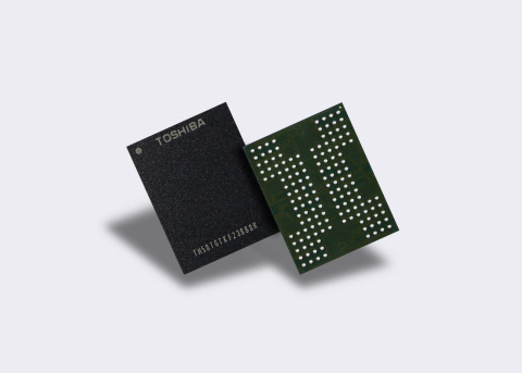
QLC 3D Flash Memory (Photo: Business Wire)
Multi-bit cell flash memories store data by managing the number of electrons in each individual memory cell. Achieving QLC technology posed a series of technical challenges, as increasing the number of bit-per-cell by one within same electron count requires twice the accuracy of TLC technology. Toshiba Memory has drawn on its advanced circuit design capabilities and industry-leading 64-layer 3D flash memory process technology to create the QLC 3D flash memory.
The prototype features the world’s largest die capacity[3] (768 gigabits/96 gigabytes) with 64-layer 3D flash memory process. Shipment of prototypes to SSD and SSD controller vendors for evaluation and development purposes started in early June.
The QLC 3D flash memory also enables a 1.5-terabyte (TB) device with a 16-die stacked architecture in a single package - the industry’s largest capacity[4]. Samples of this groundbreaking device will be showcased at the 2017 Flash Memory Summit in Santa Clara, California, United States, from August 7-10.
Toshiba Memory already mass produces 64-layer 256-gigabit (32-gigabytes) devices, and as it expands mass production it will continue to demonstrate industry leadership by advancing technology development. Focused on meeting growing demand for high density, smaller chip size flash memory solutions, the new QLC device targets such applications as enterprise SSD, consumer SSD and memory cards.
Note:
1. Source: Toshiba Memory Corporation, as of June 28, 2017.
2.
A structure stacking Flash memory cells vertically on a silicon
substrate to realize significant density improvements over planar NAND
Flash memory, where cells are formed on the silicon substrate.
3.
Source: Toshiba Memory Corporation, as of June 28, 2017.
4. Source:
Toshiba Memory Corporation, as of June 28, 2017.
• Company names, product names, and service names mentioned herein may be trademarks of their respective companies.
View source version on businesswire.com: http://www.businesswire.com/news/home/20170627006601/en/
Contact:
Toshiba Memory Corporation
Kota Yamaji, +81-3-3457-3473
Business
Planning Division
Email Contact


 Animation, 3D Art and 3D Models")